Design and Verification of DDR SDRAM Memory Controller Using SystemVerilog For Higher Coverage
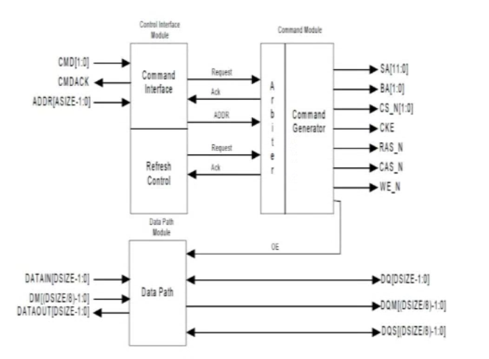 Image credit:
Unsplash
Image credit:
Unsplash
Abstract
In present electronic systems, DDR SDRAM (Double Data Rate Synchronous Dynamic Random-Access Memory) is a next-level advanced version of regular SDRAM, developed with advanced key features such as effective use of memory bandwidth and its capability to transact data on both edges of clock cycles. DDR SDRAM is widely used in computer applications like laptops, DSP processing systems, and networking. Cost and speed are two important factors in designing memories like DDR SDRAM, which meet the standards in the field of DSP applications. Because of its high speed, burst access, and pipeline feature, DDR SDRAM becomes more popular. The basic operations of the DDR SDRAM memory controller are very similar to those of the SDR (Single Data Rate) SDRAM memory controller, differing only in their circuit design. DDR uses sophisticated circuit techniques to achieve high speed and perform more operations per clock cycle. DDR SDRAM uses a double data rate architecture, meaning transactions of data occur on both the rising and falling edge of the clock cycles. The DDR SDRAM controller makes many low-level tasks, like refresh, initialization, and timings, invisible to the user. DDR SDRAM is designed with objectives like proper command use for Read/Write accesses and proper active and pre-charge commands. In this work, a DDR SDRAM controller is designed using Verilog HDL, and verification is carried out using SystemVerilog with the Questasim Tool. Functional coverage of 100% is achieved by applying randomized test cases.